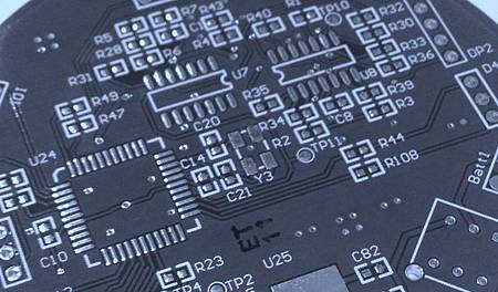
很多人在學校都使用萬用板在製作電路,
Many peple use the perfboard to assemble electrical circuit in school.
萬用板提供一個很方便的方式-只要將IC的接腳和線插到洞裡做連結即可完成,
The perfboard provide a convenient method - only plugs IC and wire into the perfborad and finishes this circuit.
不過缺點便是:無法縮小體積,以及大量生產,
But there are some disadvantages: size can't be miniaturized and produced massively.
目前工程上的方式是製作PCB板,大部分的元件是SMD封裝,再加上少許的插件。
So far, the engineering method is to fabricate PCB board, most of components are SMD package, and few are DIP package.
製作PCB的過程為:
The process of manufacturung PCB is :
1. 畫好電路圖 develop schematic file
2. 將電路圖變成PCB layout(佈線) translate schematic to PCB layout.
3. 最後請PCB廠商將PCB製作出來 finally, send gerber file to the factory, and make PCB board.
好的設計的PCB板需要可以過安規的測試,包含電性安全與電磁干擾,
The good designed pcb board has to pass regulation test including electric safety and electromagnetic interference.
這需要在電路上經驗的累積。
This needs a lot of experiences on PCB design.


 留言列表
留言列表

 {{ article.title }}